Electronic Pcb
Electronic PCB using lines, pads and other features etched from one or more sheet layers of copper laminated onto and/or between sheet layers of a non-conductive substrate. Components are generally soldered onto the PCB to both electrically connect and mechanically fasten them to it.
Alternatives to Electronic pcb include wire wrap and point-to-point construction, both once popular but now rarely used. Electronic pcb require additional design effort to lay out the circuit, but manufacturing and assembly can be automated. Electronic computer-aided design software is available to do much of the work of layout. Mass-producing circuits with Electronic pcb is cheaper and faster than with other wiring methods, as components are mounted and wired in one operation. Large numbers of Electronic pcb can be fabricated at the same time, and the layout only has to be done once. Electronic pcb can also be made manually in small quantities, with reduced benefits.
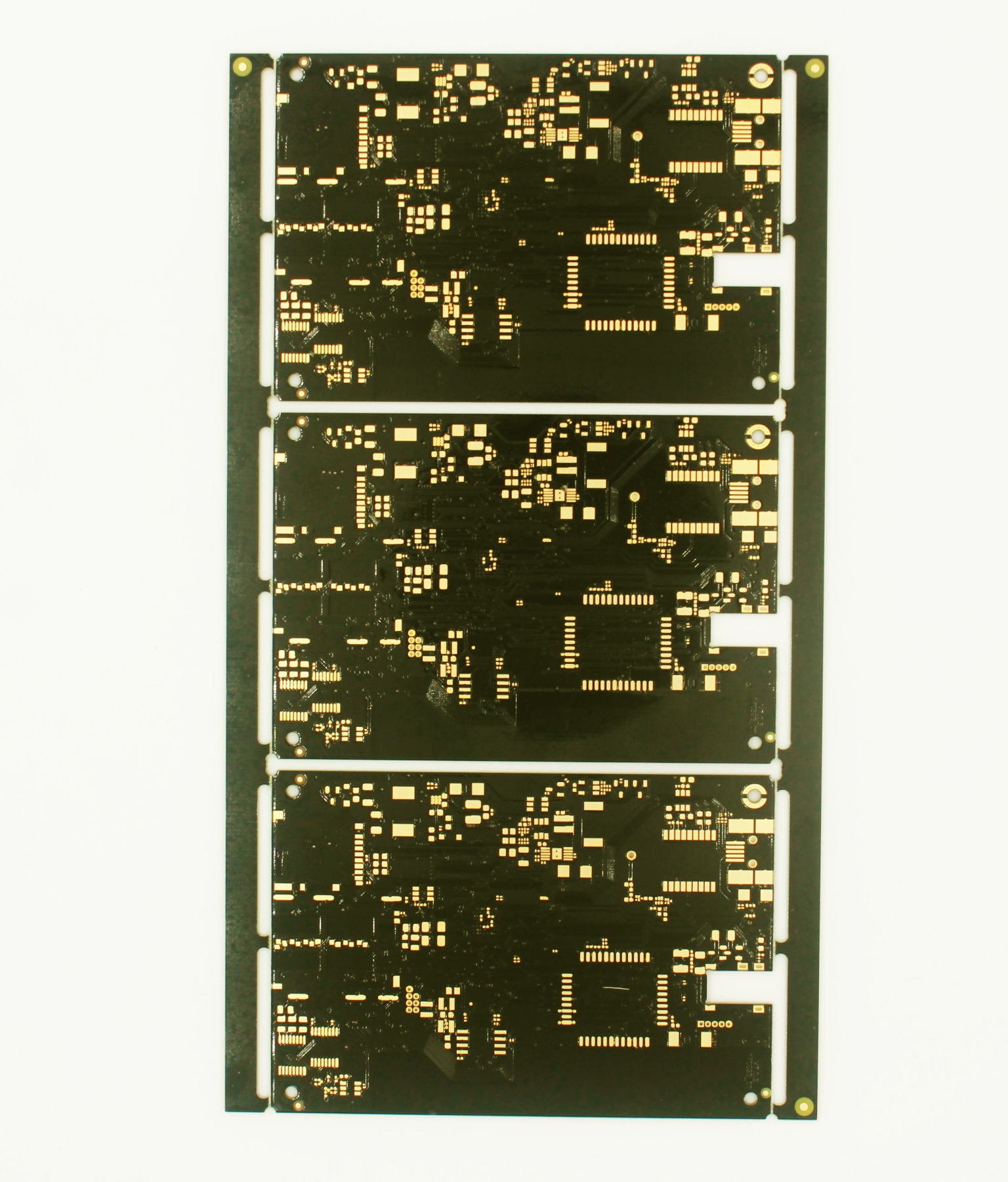
Electronic pcb can be single-sided, double-sided , or multi-layers.
single-sided: When the other side of the PCB is concentrated on the other side of the board, the components are concentrated on the other side. Because the wires only appear on one side, this PCB is called single sided. Because the single panel has many strict restrictions on the design of the circuit (because there is only one side, the wiring can not be crossed, and it must take a separate path), so only the early circuits used this kind of board.
double-sided: This kind of circuit board has wiring on both sides of the board, but to use the wires on both sides, it is necessary to have proper circuit connection between the two sides. The "bridge" between these circuits is called a via. A pilot hole is a small hole in a PCB filled with or coated with metal, which can be connected to wires on both sides. Because the area of the double-sided panel is twice as large as that of the single panel, the double panel solves the problem of staggered wiring in the single panel (it can be connected to the other side through holes), so it is more suitable for more complex circuits than the single panel.
multi-layers: In order to increase the area of wiring, multi-layer boards use more single or double-sided wiring boards. The printed circuit board (PCB) with one double-sided as inner layer, two single-sided as outer layer, two double-sided as outer layer, two single-sided as outer layer and two single-sided as outer layer are alternately connected by positioning system and insulating bonding materials, and the conductive patterns are interconnected according to the design requirements, which is also called multilayer printed circuit board. The number of layers of the board does not mean that there are several independent wiring layers. In special cases, empty layers are added to control the thickness of the board. Usually, the number of layers is even and contains the two outermost layers. Most of the motherboards are 4 to 8-layer structure, but in theory, nearly 100 layers of PCB can be achieved. Most of the large supercomputers use a fairly multi-layer motherboard. However, because this kind of computer can be replaced by many ordinary computer clusters, the super multi-layer board has been gradually abandoned. Because the layers in the PCB are closely combined, it is not easy to see the actual number, but if you carefully observe the motherboard, you can still see.